
Domestic Progress of Advanced Packaging Tools (Bonders/Molders/Grinders)
If you want to understand how serious a country is about advanced packaging and heterogeneous integration, do not just look at its wafer fabs. Look at its bonders, holders, and the investors behind them. Those quiet, often overlooked tools and capital flows tell you whether the ecosystem is really ready for 2.5D and 3D integration, chiplets, HBM, and all the other buzzwords of the AI era—or whether it is still just talking about them.
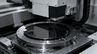
Across major semiconductor regions, domestic progress in advanced packaging tools is accelerating. Local equipment vendors are racing to close the gap with global leaders, new generations of wafer and die bonders are being installed on pilot and production lines, and investors are finally treating advanced packaging as a strategic frontier rather than a commoditized afterthought. The result is a fast-moving landscape where bonders, holders, and capital are aligning to support the next stage of heterogeneous integration.
Why Advanced Packaging Tools Suddenly Matter
For a long time, “semiconductor equipment” meant front‑end tools: lithography, etch, deposition, CMP. Packaging tended to rely on simpler, lower‑margin machines, and many countries focused on front‑end localization first. That equation has changed dramatically with the rise of:
- AI accelerators that rely on complex 2.5D/3D packages with HBM and large logic dies.
- Chiplet-based designs that demand fine‑pitch die‑to‑die connections.
- Advanced encapsulation flows such as FOWLP, panel‑level packaging, and hybrid bonding.
These architectures are only possible if the back end has extremely capable tools: wafer bonders for 3D stacks, temporary bond/debond systems for ultra‑thin wafers, fine‑pitch die bonders, precision holders and carriers, and increasingly sophisticated inspection and metrology. The bonders and holders are no longer secondary; they are the mechanical “hands” and “jigs” that make heterogeneous integration real.
In that context, domestic progress in advanced packaging tools is not just about industrial policy; it is about whether a region can take part in—and profit from—the advanced packaging revolution that now sits at the heart of AI hardware.
Bonders: The Front Line of 3D and Chiplets
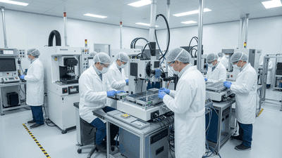
Among advanced packaging tools, bonders occupy center stage. They are the machines that physically bring wafers and dies together, aligning thousands or millions of micro‑scale pads and interconnects, and forming reliable bonds that survive years of thermal and mechanical stress. As packaging has evolved, so too has the bonder landscape, moving from simple die attach to a rich taxonomy:
- Wafer‑to‑wafer bonders for memory and logic stacking.
- Die‑to‑wafer and die‑to‑die bonders for chiplet integration and HBM assembly.
- Hybrid bonders for direct oxide‑to‑oxide plus metal‑to‑metal connections at very fine pitch.
- Thermo‑compression bonders for fine‑pitch micro‑bump interconnects in 2.5D systems.
Domestic progress is particularly visible in the push toward hybrid bonding and advanced thermo‑compression bonding. Local toolmakers are moving beyond conventional flip‑chip wire‑bonding and standard die bonders to systems that can handle:
- Sub‑micron alignment accuracy.
- Ultra‑thin wafers and fragile 3D stacks.
- Multi‑step processes with in‑situ cleaning, plasma activation, and controlled pressure and temperature ramps.
These capabilities are essential for stacking logic and memory at high density and for integrating chiplets with the kind of bandwidth and energy efficiency that AI and HPC workloads demand. When domestic bonders reach production‑class performance in these regimes, it is a strong sign that a country’s advanced packaging ecosystem is maturing rapidly.
Holders, Carriers, and the “Invisible” Precision Layer
If bonders are the hands of advanced packaging, holders and carriers are the bones. They provide the mechanical foundation that allows wafers and dies to be processed, aligned, thinned, bonded, and reworked without cracking, warping, or misaligning. As wafer thickness drops and 3D stacks grow taller and more complex, these seemingly simple components become critical.
Domestic progress in holders and carriers takes several forms:
- Development of carrier wafers and glass panels for temporary bonding and debonding flows.
- Design of precision chucks, clamps, and vacuum interfaces that maintain planarity and minimize stress.
- Specialized holders for panel‑level packaging, where large substrates require very tight dimensional control.
- Mechanically robust yet thermally optimized fixtures for high‑temperature bonding and reflow steps.
In advanced packaging lines, yield can hinge on whether a wafer stays perfectly flat during bonding or whether a temporary carrier releases cleanly after thinning. Domestic vendors that master this “invisible” precision layer play a crucial role in reducing dependency on imported fixtures and in raising overall packaging yield and reliability. It is not glamorous, but it is foundational.
Domestic Toolmakers: From Followers to Co‑Innovators
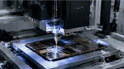
The global market for advanced bonders and related tools has long been dominated by a handful of international companies. For domestic suppliers, the challenge has been to move from trailing positions in mature, lower‑end segments to serious contenders in leading‑edge flows:
- Hybrid bonding equipment compatible with next‑generation memory and logic stacks.
- Wafer bonders for 3D image sensors, CIS, and advanced memory.
- Thermo‑compression bonders for 2.5D GPU and AI accelerator packages with HBM.
- Temporary bond/debond systems optimized for ultra‑thin wafer handling in 3DICs.
Domestically, we are starting to see:
- Toolmakers that previously served front‑end markets extend their know‑how into advanced packaging, repurposing expertise in etch, deposition, or lithography for redistribution layers and wafer preparation.
- Equipment startups focusing purely on packaging, with targeted product lines such as die‑to‑wafer hybrid bonders or panel‑level bonders.
- Collaborations between domestic OSATs and equipment vendors, co‑developing tools tuned to local 2.5D/3D and chiplet roadmaps.
The interesting shift is qualitative: domestic bonders are no longer just lower‑cost alternatives for mature technologies; they are increasingly designed with cutting‑edge packaging flows in mind, aiming to be first‑class citizens in 3DIC and heterogeneous integration lines.
Policy and Strategic Drive Behind Localization
Few factors have accelerated domestic progress more than the realization that advanced packaging is now a strategic chokepoint. When AI chips cannot ship because of a lack of HBM bonding capacity or because advanced packaging slots are fully booked abroad, it becomes clear that relying on foreign tools and lines is a real risk.
In response, many governments and regional blocs have:
- Designated advanced packaging and assembly equipment as critical technologies for national security and economic resilience.
- Launched funding programs aimed at joint R&D centers for packaging tools and integration flows.
- Offered incentives for domestic OSATs and foundries to adopt local equipment in new 2.5D/3D and chiplet lines.
These policies do two things at once: they mitigate supply chain risk and they create a protected market segment where domestic toolmakers can gain experience and scale. It is not about shutting out foreign vendors, but about ensuring that domestic players have enough opportunity and runway to progress from prototypes to full‑scale production tools.
Investors: From Skepticism to Strategic Focus
For years, many investors considered semiconductor equipment—especially backend tools—too cyclical, too niche, or too dominated by incumbents to be attractive. That sentiment is changing fast. As advanced packaging becomes a key bottleneck and profit pool, investors are paying much closer attention to domestic bonders, holders, and related tool companies.
Three shifts stand out in the investment landscape:
- Longer time horizons. Investors recognize that developing world‑class bonders is a multi‑year journey. Capital is increasingly structured to support sustained R&D rather than short product cycles.
- Strategic partnerships. Investment deals often involve not just financial capital but strategic customers—domestic foundries, OSATs, and large chip design houses—who commit to co‑development or pilot deployments.
- Portfolio depth. Instead of backing a single “champion,” investors build portfolios across the tool chain: bonders, debonders, metrology, cleaning, and advanced carriers, creating an ecosystem of domestic suppliers.
This investment behavior signals a structural belief: advanced packaging is not a temporary bubble driven by one AI cycle; it is a durable shift in how semiconductors will be built for the next decade or more. Investors want a seat at that table.
Case Study Archetypes: How Progress Looks in Practice
Even without naming specific companies, we can sketch some common archetypes of domestic progress in advanced packaging tools. These patterns show up repeatedly in different countries and regions.
1. The Front‑End Veteran Turned Packaging Innovator
This is the toolmaker that built its reputation on front‑end equipment—say, cleaning, deposition, or precision motion systems—and is now extending its platform into packaging. It already knows how to build ultra‑clean systems, precise temperature control, and high‑throughput automation. By adding modules for wafer bonding, debonding, or fan‑out molding, it becomes a serious domestic supplier for advanced packaging flows.
Often, these companies:
- Leverage existing relationships with local fabs to pilot new packaging tools.
- Offer integrated lines that combine front‑end‑style process control with back‑end assembly steps.
- Move quickly into high‑growth niches like 3D memory stacking or CIS packaging.
2. The Specialized Bonder Startup
Another archetype is the focused startup that aims squarely at one or two advanced bonding technologies: for example, hybrid bonding or D2W thermo‑compression bonding for 2.5D/3D AI packages. These companies are typically small but deeply technical, often founded by engineers from global tool vendors or advanced packaging houses.
Their progress is usually marked by:
- Demonstration of a single flagship tool at a domestic OSAT or R&D line.
- Rapid iteration on alignment accuracy, throughput, and yield metrics.
- Gradual expansion into adjacent tools like inspection or alignment metrology once the core bonder gains traction.
Investors like these startups because they can become technology leaders in narrow but crucial segments of the tool chain.
3. The Panel‑Level Packaging Pioneer
As fan‑out panel‑level packaging (FOPLP) gains momentum, a third archetype emerges: the domestic vendor that focuses on large‑format panels instead of round wafers. This plays to local strengths in flat panel, glass, or mechanical engineering.
Such companies typically pursue:
- Panel bonders and handlers designed for large substrates used in FOPLP.
- Precision panel carriers and holders that control warpage and dimensional drift.
- Integrated lines combining molding, RDL, and mounting and bonding for system‑in‑package modules.
For heterogeneous integration, panel‑level packaging offers a path to lower cost and higher throughput once processes mature. Domestic toolmakers in this area can help their regions leapfrog directly into high‑volume panel‑based packaging for mobile, automotive, and consumer AI applications.
How Domestic Progress Changes the Heterogeneous Integration Game
Domestic mastery of bonders, holders, and related tools is not just about replacing imports. It has direct consequences for how heterogeneous systems are designed and manufactured locally.
- Shorter iteration cycles. When equipment is local, packaging houses and chip designers can work more closely with tool vendors to tweak processes, try new stack architectures, and optimize for yield and performance.
- More customized flows. Domestic toolmakers can tailor bonders and carriers to local design rules, substrate choices, and chiplet standards, rather than adapting generic global platforms.
- Better alignment of roadmaps. Interactions between domestic chip design, OSATs, and equipment companies ensure that tool capabilities evolve in lockstep with heterogeneous integration roadmaps—whether that means more chiplets, thicker stacks, or larger substrates.
Ultimately, this can produce packaging solutions that are differentiated, not derivative—local ecosystems that innovate on architecture and process, rather than simply copying global reference flows.
Challenges on the Road to Domestic Maturity
Of course, domestic progress is not without hurdles. Several persistent challenges stand between early success and global competitiveness:
- Global incumbents. Established toolmakers have deep process know‑how, broad product portfolios, and strong relationships with leading fabs and OSATs. Catching up requires sustained effort, not just one or two tool generations.
- System complexity. Advanced bonders are complex mechatronic systems with optics, high‑precision motion, control software, and process chemistry. Building all of that domestically at world‑class levels takes time.
- Volume and learning curves. Tool performance improves with field experience. Domestic vendors need sufficient volumes and diverse deployments to drive learning and refinement.
- Talent and ecosystem. It is not enough to have good hardware; domestic progress also depends on metrology companies, materials suppliers, and a pipeline of engineers who understand both front‑end and back‑end physics.
That said, the momentum is clearly shifting. The combination of policy support, market demand from AI and heterogeneous integration, and growing investor interest is creating a window in which domestic toolmakers have a genuine chance to move from catch‑up to co‑leadership.
Conclusion: Tools, Trust, and the Future of Advanced Packaging
The story of domestic progress in advanced packaging tools—bonders, holders, and the investors backing them—is ultimately a story about trust and capability. Can a country trust its own ecosystem to assemble the most complex AI and 3DIC systems it designs? Can it rely on local tools to keep up with the relentless pace of heterogeneous integration?
As domestic toolmakers roll out hybrid bonders, thermo‑compression systems, advanced carriers, and panel‑level equipment, and as investors take the long view on advanced packaging, the answer increasingly looks like “yes.” The advanced packaging revolution is not only about new architectures and materials; it is about building the domestic tools and capital structures that allow those innovations to scale. In that sense, the quiet progress in bonders and holders may turn out to be one of the most decisive factors in who leads—and who follows—in the era of advanced packaging and heterogeneous integration.
You May Like

Narrowing Spread Between NAND Spot and Contract Prices in 2026 – A Signal
By 2026, one of the most watched metrics in the NAND flash market has started to shift in a subtle but meaningful way: the spread between spot prices and long‑term contract prices is narrowing. For casual observers, this may look like just another incremental change in a notoriously volatile industry. For memory makers, module houses, device OEMs, and data center buyers, however, a tightening gap between spot and contract prices is a signal—a reflection of evolving supply–demand balance, risk perceptions, and strategic behavior on both sides of the market.

Price Divergence Trading Strategies Between NAND Flash and DRAM ETFs
NAND flash and DRAM sit at the core of AI storage and computing power. Both are memory, but they are not the same business. DRAM is main memory—fast, volatile, and central to high‑bandwidth workloads like AI training and inference. NAND is non‑volatile storage—slower than DRAM, but crucial to persistent data and large‑scale object storage. The cycles that drive their pricing and margins overlap, yet they often diverge. That divergence is where trading strategies between NAND and DRAM ETFs become interesting.

China’s HBM Localization Progress: The Catch-Up Pace of CXMT and XMC
China’s drive to localize advanced memory technologies has accelerated over the past several years. High-Bandwidth Memory (HBM) sits near the center of that strategy because it is integral to AI accelerators, high-performance computing (HPC) and other strategic compute platforms. Two domestic players—ChangXin Memory Technologies (CXMT) and XMC (Xianghui Memory, commonly referred to as XMC)—have become focal points in assessing how quickly China can close the gap with international incumbents on HBM die, stacking, and packaging.

Thermal Simulation Challenges and Solutions in 3DIC AI Chip Design
As AI workloads push chips to deliver ever higher compute density, designers are increasingly turning to three‑dimensional integration (3DIC) to stack dies vertically and pack more functionality into limited footprints. While 3DIC architectures unlock significant performance and bandwidth advantages, they also introduce complex thermal behaviors that are far harder to predict and manage than in traditional 2D layouts.

An Attempt at Compiling a Memory+Compute Fusion Thematic Index – A Dual-Track Framework
Most AI investors talk about “compute” as if it were the whole story: GPUs, accelerators, chips, cores. But every one of those cores needs somewhere to read from and write to. Memory and storage define how wide the data highway really is. In practice, AI performance is a fusion of compute and memory, not a solo act. So why do so many indices and ETFs separate them into different silos—one for semiconductors, one for memory, one for data centers—when the actual workloads keep blending them?
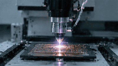
Surging Demand for Laser Drilling and Plasma Dicing Equipment in Advanced Packaging
Advanced packaging has become one of the semiconductor industry’s most important growth engines, and it is now pulling a surprising set of process tools into the spotlight. Among the most in-demand are laser drilling and plasma dicing equipment. These machines sit close to the heart of heterogeneous integration, fan-out packaging, wafer thinning, TSV formation, glass substrate processing, and other advanced flows where precision, yield, and throughput matter enormously. As packaging moves from a back-end afterthought to a strategic platform, the equipment used to shape, open, and separate materials has become just as important as the dies themselves.

D2D Interface Bandwidth and Latency Comparison in Chiplet Architectures
Chiplet architecture has turned the package into a real performance battleground. Once multiple dies are placed side by side or stacked within the same advanced package, the quality of the die-to-die, or D2D, interface becomes one of the most important determinants of system behavior. Bandwidth is no longer a nice-to-have metric, and latency is no longer a small implementation detail. Together, they shape whether a chiplet system feels nearly monolithic or frustratingly fragmented.

Stock Selection Logic and Alpha Validation of ESG-Themed Semi ETFs
Semiconductor themed ETFs are no longer just about growth and cycles. A growing subset now layers environmental, social, and governance (ESG) criteria on top of traditional sector exposure. These ESG semi ETFs promise two things at once: access to one of the market’s most powerful secular themes, and alignment with sustainability and governance standards. The pitch is appealing, but it raises two hard questions. First, how exactly are these stocks being selected? Second, does the ESG overlay help, hurt, or leave alpha unchanged?